1. Solution Overview
1.1 Industry Background
Micro-nano lithography is a core process for PCB fabrication, microfluidic chips, MEMS devices and precision micro-structure mold processing. As feature linewidth continues to shrink, exposure systems require light sources to provide uniform beams, stable wavelengths, consistent power, and high modulation speeds.Fiber-coupled semiconductor lasers feature easy integration and flexible control, and have become preferred laser light source solution for LDI direct imaging, dry-film lithography and SU-8 thick photoresist exposure.
1.2 Compatible Wavelengths
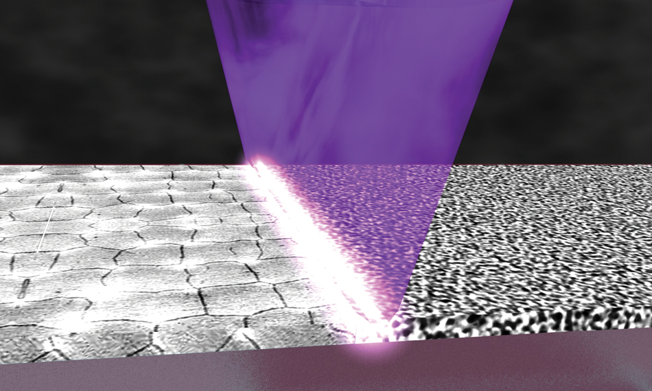
375nm and 405nm near-UV fiber-coupled laser modules are widely used in lithography. 375nm offers higher photon energy for high-resolution micro-patterning, while 405nm balances reliability and lifespan for mass PCB production. Wavelength selection depends on photoresist type and resolution target.
2. Core Advantages
2.1 Stable Wavelength for Consistent Yield
Integrated TEC temperature control and constant-current driver minimize wavelength drift caused by temperature variation. Low power fluctuation and good batch consistency help avoid blurred patterns and uneven resolution.
2.2 Flexible Fiber Delivery for Lithography Optical Layout
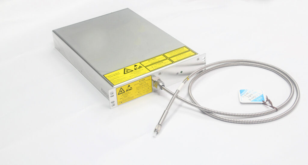
Single-mode and multi-mode fiber options with FC/SMA connectors. The laser body can be installed remotely from the exposure plane, easy to integrate with galvanometers and motion stages, simplifying optical alignment for OEM equipment.
2.3 High-Speed Modulation for Scanning Exposure
TTL modulation and analog power adjustment are supported with fast response, suitable for LDI scanning systems. On-demand light output prevents over-exposure and improves throughput.
3. Typical Application Scenarios
3.1 PCB LDI Direct Imaging
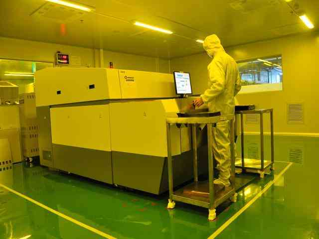
Exposure for single/double-sided PCB circuits, solder mask and dry film, compatible with mainstream PCB photoresists for mass production.
3.2 Microfluidic & MEMS Lithography
SU-8 thick resist patterning, micro-channel and micro-sensor fabrication for R&D and low-volume high-end component manufacturing.
3.3 Photomask Replication & Micro-Mold Lithography
High-precision mask duplication and fine texture mold machining for optics and semiconductor auxiliary parts.
4. Customization & Technical Service
4.1 Customizable Specifications
Optical power, fiber core, NA, modulation frequency and power supply can be customized. Multi-channel combined light sources are available upon request.
4.2 Full Technical Support
Optical test reports, beam profiling data and driver references are provided. And,we support prototype joint testing and lithography process verification, together with export documentation.
5. Cooperation
We supply375nm & 405nm fiber-coupled violet laser modules dedicated to lithography. With in-house packaging and optical testing facilities, our product portfolio also includes 395nm,450nm, 638nm,650nm, 660nm, 780nm ,808nm 940nm, 850nm, 980nm lasers. Sampling, pilot run and mass delivery are available. Lithography equipment makers and research institutes are welcome for custom exposure light source solutions.


Add comment