1. What is LDI Technology?
LDI, the full name of Laser Direct Imaging, is a digital maskless lithography technology that has completely replaced traditional film exposure processes in high-end printed circuit board manufacturing, covering rigid PCB, flexible FPC, HDI boards and IC packaging carrier boards. Traditional PCB exposure processes utilize physical photomask films. These films block light to transfer circuit patterns onto photoresist coated over substrates. This process inevitably brings multiple defects such as film thermal expansion and contraction deviation, surface dust pollution, film scratches and high film production costs.
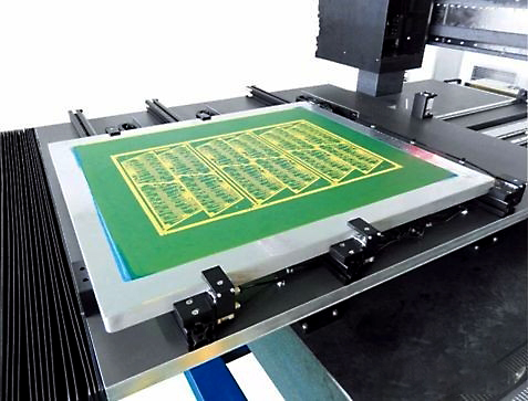
Different from the traditional process, LDI directly imports digital circuit files including Gerber and ODB++ into the equipment control system, converts graphic data into controllable laser light signals, and accurately projects tiny laser spots onto the photoresist layer of the board to complete selective exposure without any intermediate mask film. This digital manufacturing method greatly optimizes production flexibility, processing precision and product yield, and has become the standard production configuration for mid-to-high-end circuit factories worldwide.
LDI
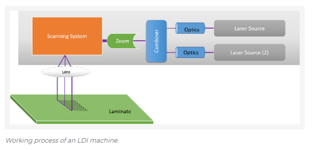
LDl is a printed board patterning process that uses a laser to directly transfer digital circuit images onto a photoresist-coated substrate using a laser, eliminating the need for phototools. It represents an advanced stage in the evolution of circuit board photolithography, offering higher accuracy and flexibility.
The machine raster-scans the substrate section by section and selectively irradiates the photoresist with the laser beam.The image formed can be comparedto the image on a CRT screen, formed from several lines across the screen.
Like traditional photolithography, LDI systems utilize photoresist. Manufacturers specially formulate this resist for laser printing, and it reacts much faster than standard photoresist.The resist comes in dry film and liquid options, with the resist application methods being identical to those used in photolithography.
What are the steps involved in the LDl process?
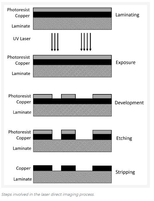
The LDl follows a sequence of surface preparation, resist coating, digital exposure, and etching. Each step ensures precise pattern transfer and minimal variation, which is critical for high-density circuit designs.
Here’s the procedure:
1. Scrubbing: This includes removing any oxide layers on the core surface using anti-oxidant baths and mechanical scrubbing with abrasive pads.
Operators use isopropyl alcohol to wipe off organic residues and oil stains on the core surface.
2. Lamination photoresist: The board panel is coated with a layer of photosensitive material.
3. Loading CAM files: CAM files are then loaded into the laser.
4. Laser printing: The circuit pattern is printed onto the board by the CNC laser.
- Etching: We use acid to etch away any photoresist areas untouched by the laser beam and retain the target circuit traces.
6. Photoresist strip: Removal of the photosensitive material
7. Drying: Drying the core/CCL after removal of photo material
Core Advantages of LDI
- No physical film needed: Cut film production, storage and replacement costs, eliminate dimensional deviation caused by film thermal expansion & contraction.
- Ultra-high precision: Minimum achievable line width/spacing down to 6–20μm, overlay alignment accuracy up to ±0.5μm, perfectly matching HDI, high-density flexible circuit and chip packaging substrates.
- Flexible rapid switching: Modify production patterns by updating digital files only, ideal for small-batch, multi-variety orders.
- Higher production yield: Avoid scratches, dust and registration errors brought by film contact exposure.
2. Which Lasers Are Used for LDI Machines?
Industrial LDI production equipment adopts UV and violet semiconductor lasers as core light sources. Their photon energy effectively triggers chemical cross-linking of dedicated PCB photoresist. We deploy lasers with distinct wavelengths for diverse production scenarios based on precision requirements, cost budgets and photoresist categories:
- 355nm solid-state ultraviolet laser. It belongs to short-wavelength high-precision light source, with ultra-small focusing spot and ultra-high monochromaticity. The system achieves sub-5μm line width imaging resolution. It perfectly fits ultra-fine IC carrier boards and premium HDI products that demand extremely high machining precision. Yet its equipment and follow-up maintenance costs remain high. Factories deploy it only for high-value advanced packaging lines.
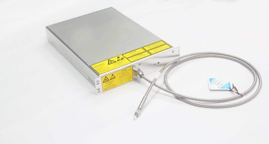
- 375nm fiber-coupled violet laser module. It strikes a perfect balance between exposure precision, service life and overall equipment cost. And, its wavelength absorption curve suits most FPC liquid photoresist and thin dry films. It features outstanding beam uniformity. This property guarantees uniform line edge roughness in mass FPC manufacturing. Medium and high-end flexible circuit manufacturers widely choose this equipment.
- 405nm fiber-coupled violet laser module. This is the most widely used light source for mass-production LDI machines. It is also our core laser tailored for LDI industry customers. The 405nm diode laser outperforms the 355nm solid laser in many ways. It consumes less power and generates less heat. It boasts longer continuous service life and lower purchase cost. It works with all mainstream PCB exposure materials, including inner dry film, outer liquid photoresist and solder mask ink. Customized power from 300mW to 12W is available, with stable power fluctuation within ±2%, supporting 24-hour uninterrupted industrial operation.
- Special alternative: 1064nm infrared laser. This laser lacks enough photon energy for standard UV photoresist. It only fits custom IR photoresist for special thick copper PCB work. It offers low precision and supports few material types, so few factories use it on mainstream LDI production lines.
Laser for LDI
Our company provides customized fiber-coupled 375nm & 405nm violet laser modules exclusively for LDI equipment. Every laser module features an integrated constant temperature driver and power closed-loop control system. It suppresses power drift and light decay during long scanning exposure. It provides steady energy for consistent PCB digital imaging.
BU-LASER is the original manufacturer of laser diode module from 375nm to 980nm, providing you with high-quality OEM & ODM services with over 16 years of mature experience!
Add comment